Summary:
UCLA researchers in the Department of Electrical and Computer and Engineering have introduced a scalable and rapid bonding method for dielet assembly on advanced packaging constructs, achieving a remarkable throughput of over 1100 units-per-hour, or 10-fold higher than the conventional assembly method.
Background:
In semiconductor packaging, effectively addressing the challenges of optimizing processor-to-memory bandwidth and memory capacity in a cost-efficient manner is paramount. Package scaling, made possible by decreasing the bump-to-bump pitch, becomes essential to fulfill the increasing requirements of high-performance computing applications. Lowering bump pitches to 10 micrometers and below has the potential to offer several terabytes of processor-to-memory bandwidth. However, this potential is currently limited to silicon-based substrates that employ two bonding methods: hybrid bonding and thermal compression bonding (TCB). Hybrid bonding demands strict processing requirements and meticulous control of dielectric roughness and metal recess, making it susceptible to particles and roughness during assembly. Meanwhile, TCB is relatively cost-effective and simpler, but it exhibits a low throughput of approximately 90 units-per-hour. Additionally, it must be executed in a single bonding step to meet the required military standard shear strength (MIL-STD 883), and the recommended die/dielet tacking process in TCB takes at least 30 seconds, rendering it less appealing from the perspective of high-volume manufacturing. Consequently, there is a compelling need for innovative approaches to enhance high-volume manufacturing capabilities, aligning with the demands of modern computing applications.
Innovation:
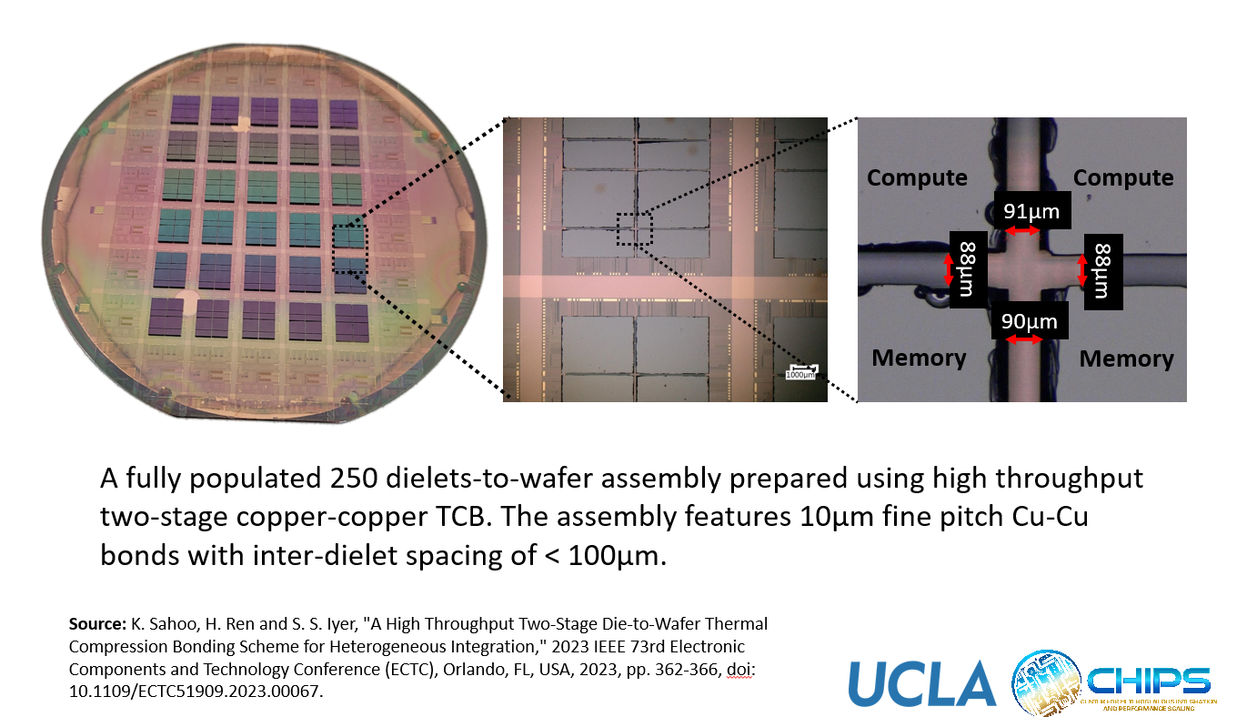
Under the guidance of Professor Subramanian Iyer, a team of researchers has developed an innovative methodology to enhance throughput for face-to-face heterogeneous dielet bonding. This invention employs a 2-stage bonding approach, combining dielet tacking and assembly-level annealing. The optimization of the tacking stage has resulted in a tacking time within 10 seconds per dielet, and the proposed approach has the capability to increase overall throughput by over 10X to more up to 1100 units-per-hour. Additionally, it ensures military standard mechanical and electrical reliability. Notably, the methodology does not distinguish between die/dielets and can be scaled to accommodate any silicon-interposer, regardless of size. Furthermore, a 2-stage high-throughput thermal compression bonding has been successfully demonstrated using a wafer-scale advanced packaging substrate and was extended to another silicon-interposers, irrespective of the size. This innovative approach holds significant promise for advancing semiconductor packaging capabilities, ushering in a new era of high-throughput, reliable bonding processes.
Potential Applications:
• Advanced packaging constructs
• Dielet assembly on interposers
• Wafer-scale packaging
• High-performance computing applications
Advantages:
• Increase throughput by over 10X, > 1100 units-per-hour
• Tacking optimization within 10 seconds
• Ensure military standard shear strength, high mechanical and electrical reliability
• Flexibility, scales for any silicon-interposer
Development to Date:
First successful demonstration of the invention: May 30th, 2023
Related Papers:
Sahoo, Krutikesh, Haoxiang Ren, and Subramanian S. Iyer. "A High Throughput Two-Stage Die-to-Wafer Thermal Compression Bonding Scheme for Heterogeneous Integration." 2023 IEEE 73rd Electronic Components and Technology Conference (ECTC). IEEE, 2023.
Reference:
UCLA Case No. 2023-144
Lead Inventor:
Prof. Subramanian S. Iyer.