Summary:
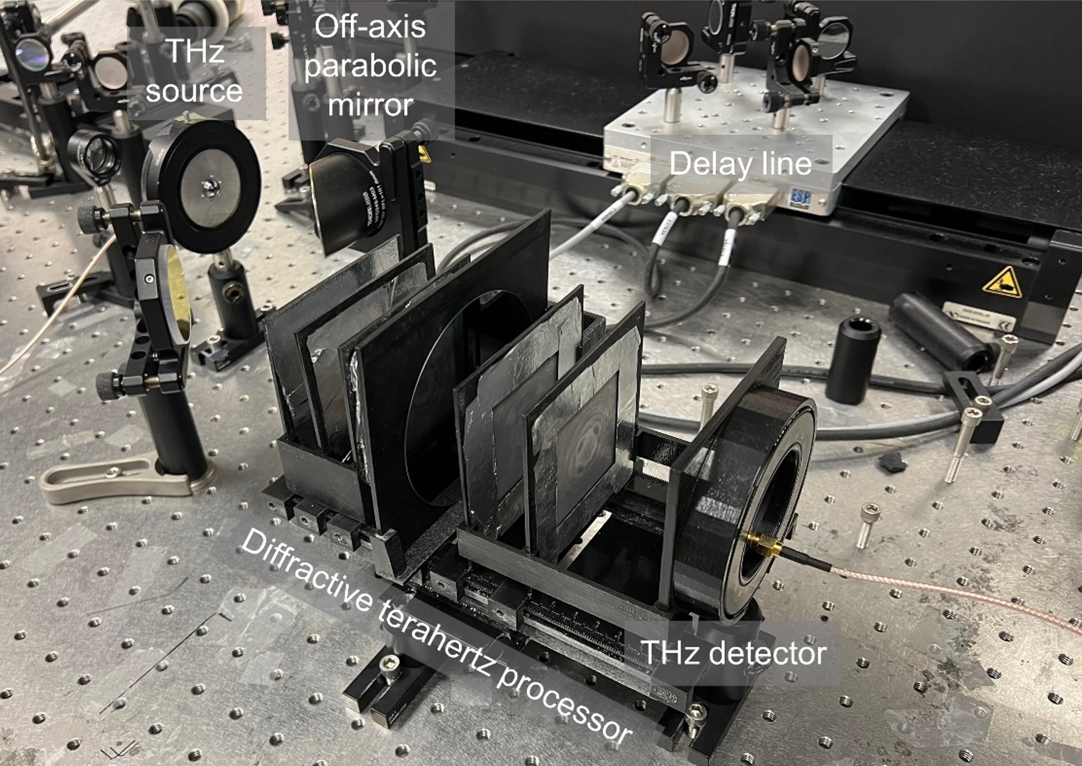
UCLA researchers have developed a diffractive sensor that leverages deep-learning-optimized diffractive layers to rapidly detect hidden objects and defects within a 3D sample without scanning or image processing.
Background:
Inspecting hidden structures is a critical requirement in various fields, including security, manufacturing, and medicine. Terahertz-based, non-invasive systems show promise towards this end; they penetrate most opaque materials and can identify their internal structural makeups. While terahertz systems have been successfully employed in quality control applications, existing systems are slow and offer relatively low signal-to-noise ratios. Optical processes that speed up object detection require bulky and expensive lasers to match the required efficiencies. Overall, the types of information that can be acquired by current systems are limited, and time and frequency-resolved data are not provided. Aside from detection limitations, feature identification is bottlenecked by the large amount of digital storage, data, and image processing needed for existing terahertz imaging systems.
Innovation:
UCLA researchers have developed an optically diffractive processor that can rapidly inspect a sample using terahertz radiation. Unlike traditional systems, this technology is entirely optical, obviating the need for image transmission, storage, and processing, thereby greatly simplifying and accelerating the defect detection process. Additionally, passive optical components eliminate the need for an external power source, except for the illumination and single-pixel detector. A machine learning algorithm, when coupled with the terahertz radiation, is used to create sample-specific defect detectors which can identify material deviations even when fully obfuscated by an opaque sample. This technology can also be applied to other frequency bands such as infrared and X-ray, further expanding its detection capabilities. Ultimately, this diffractive processor will be useful in fields where high-throughput material screening and inspection is critical. Unlike conventional imaging-based methods, which are often hindered by 3D image data overload, this defect detection approach can deliver markedly higher sensing throughput while offering cost-effectiveness and simplicity.

Potential Applications:
• Security screening.
• Biomedical sensing.
• Industrial quality control.
• Anti-counterfeiting measures.
• Historical artefact preservation.
Advantages:
• Simplified and accelerated defect detection.
• Cost effective.
• Eliminates need for external power source, except for the illumination and single-pixel detector..
• No image processing required.
• No data transmission or storage required.
• Eliminates need for focal plane array and raster scanning.
• Can be applied to any wavelength in electromagnetic spectrum.
State of Development:
The inventors have designed and experimentally validated the technology, successfully detecting hidden objects inside of silicon samples. The technology has been published in a peer-reviewed academic journal.
Related Publications:
1. Li, J., Li, X., Yardimci, N.T. et al. Rapid sensing of hidden objects and defects using a single-pixel diffractive terahertz sensor. Nat Commun 14, 6791 (2023). https://doi.org/10.1038/s41467-023-42554-2
Information-hiding cameras: Optical concealment of object information into ordinary images. SCIENCE ADVANCES
12 Jun 2024, Vol 10, Issue 24, DOI: 10.1126/sciadv.adn9420
Reference:
UCLA Case No. 2023-184
Lead Inventor:
Aydogan Ozcan, UCLA Professor of Electrical and Computer Engineering